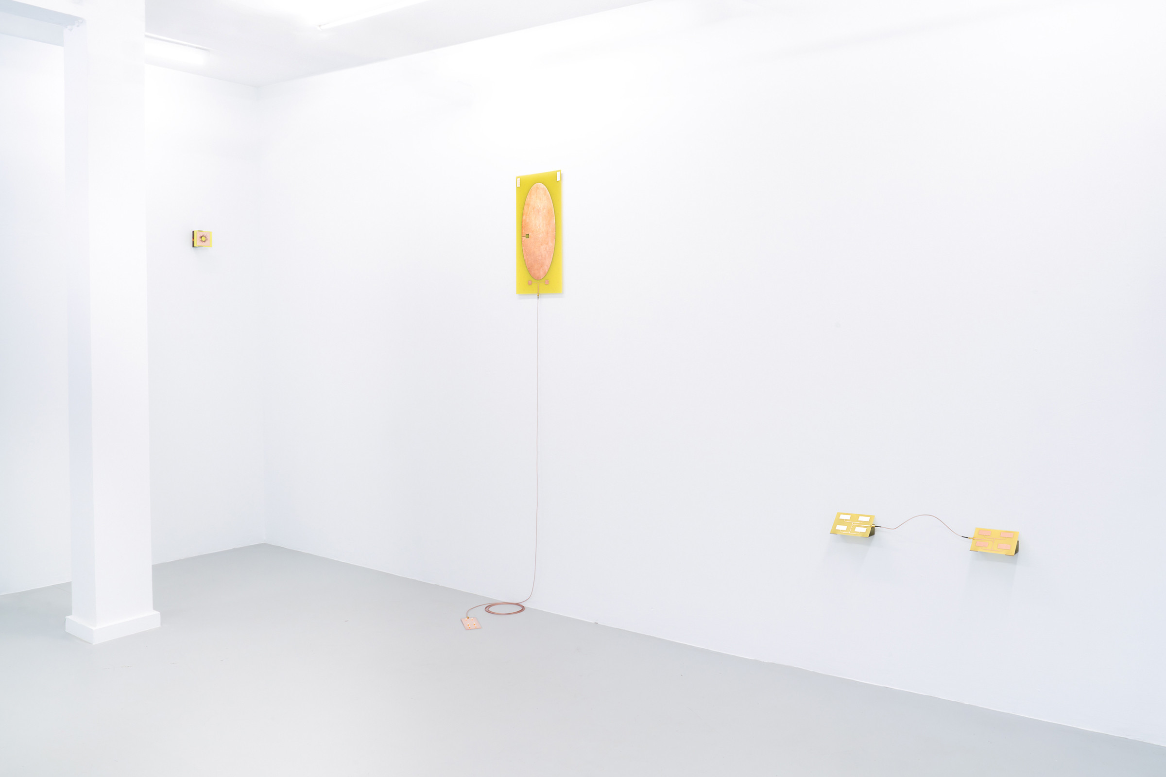
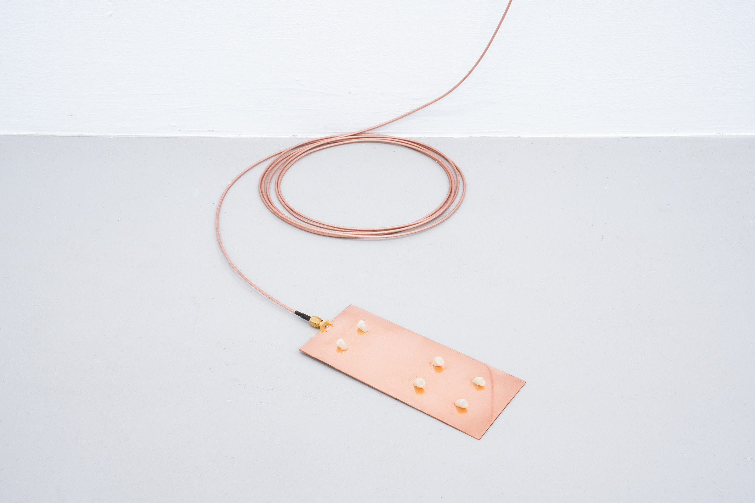
PCBs, SMA cable, PCB Board, copper, resin teeth, faux eye lashes, SMD GPS GLONASS Antenna, mild steel brackets, 2023
Fishy Business, group exhibition at Five Years, London, UK
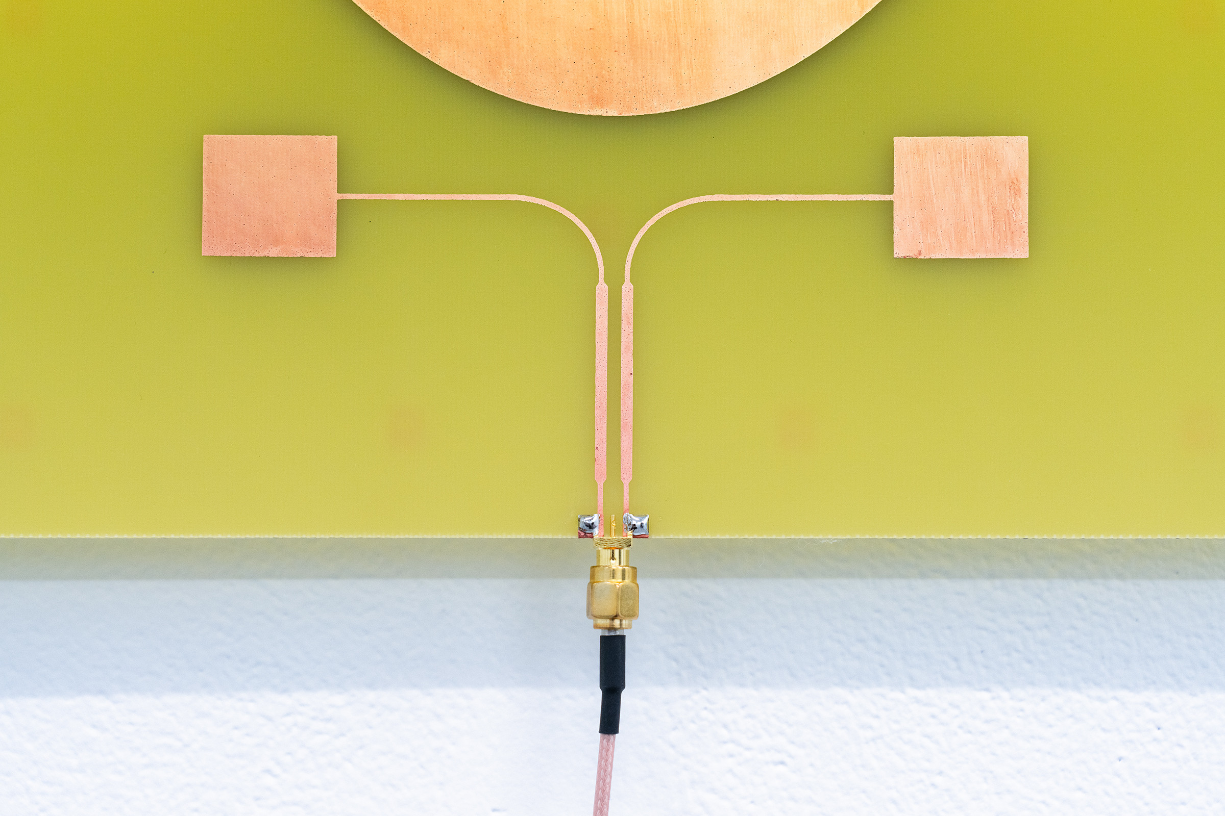
Microwave, PCB Board, SMA cable, copper, resin teeth 50 x 222 x 48cm, 2023
Fishy Business, group exhibition at Five Years, London, UK
Microwave, PCB Board, SMA cable, copper, resin teeth 50 x 222 x 48cm, 2023
Fishy Business, group exhibition at Five Years, London, UK
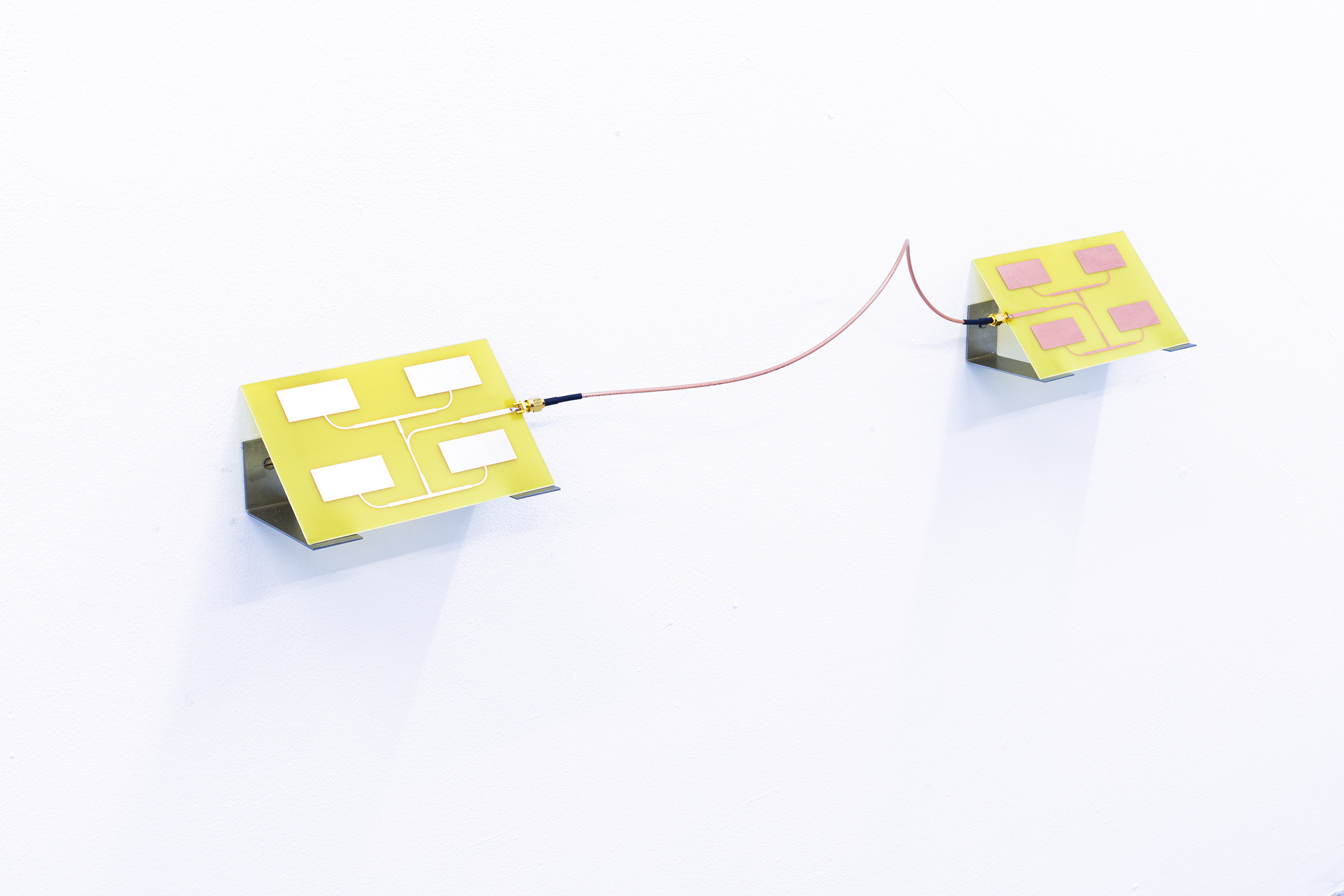
Radiator, PCB board, SMA cable, mild steel brackets, 72 x 8 x 7.5cm, 2023
Fishy Business, group exhibition at Five Years, London, UK
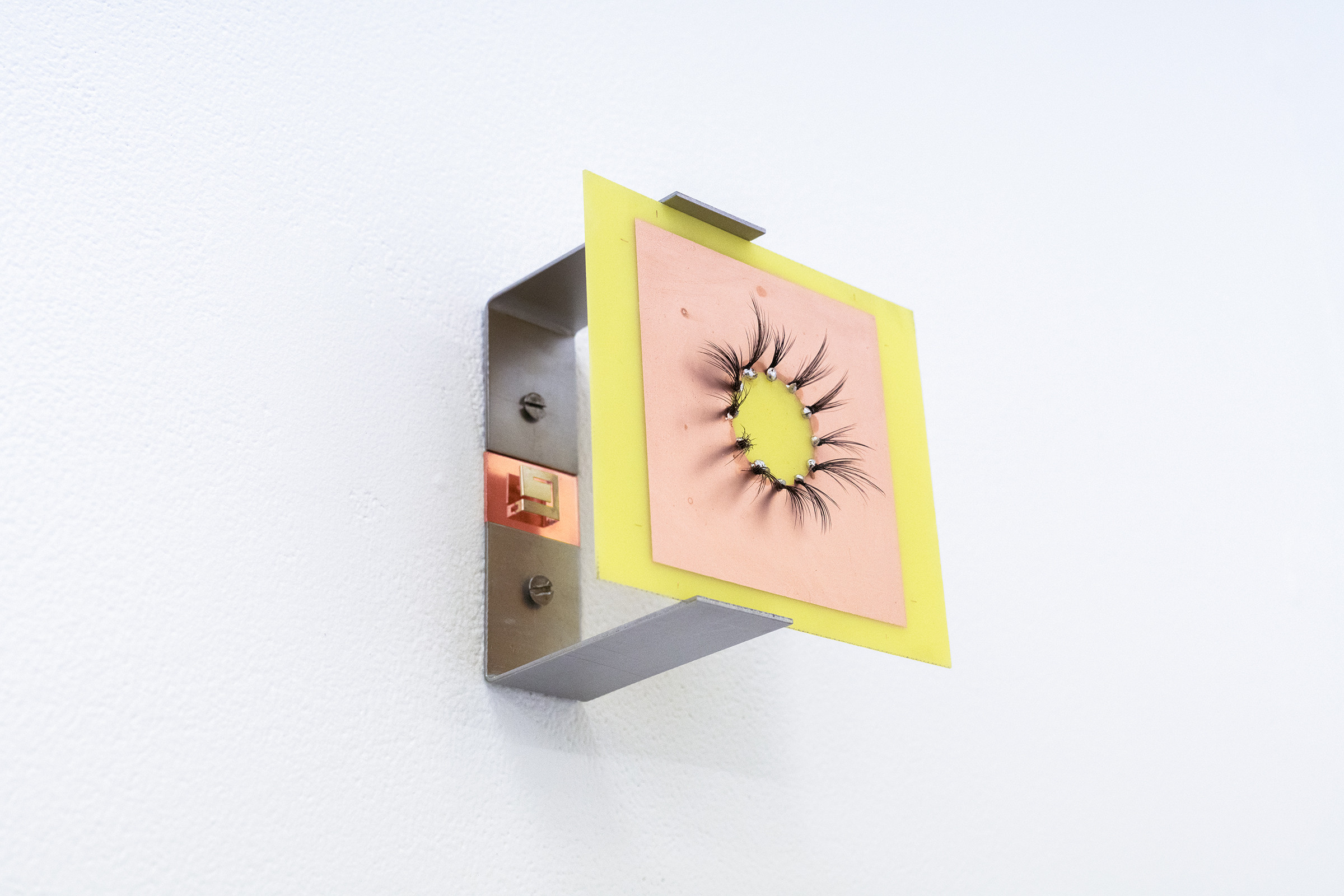
Television, PCB board, faux eye lashes, mild steel brackets, SMD GPS GLONASS Antenna, 12 x 10.5 x 7cm, 2023
Fishy Business, group exhibition at Five Years, London, UK